Heterogeneously Integration
Heterogeneous integration bonds unpatterned III-V thin films to silicon wafers at the early- to mid-stages with a coarse alignment, and then define devices lithographically on the full wafer scale.
Overview
Heterogeneous integration bonds unpatterned III-V thin films to silicon wafers at the early- to mid-stages with a coarse alignment, and then define devices lithographically on the full wafer scale. This technique allows for versatile management of the gain materials for the best achievable on-chip performance. A notable example is using QD active region for lower threshold current density, higher temperature stability, defect insensitivity, better immunity to fabrication defects, and reduced reflection sensitivity. Device design and process optimization have been actively conducted to replace InP-based quantum well (QW) epitaxial material with GaAs-based QD epitaxial material, in our latest results, robust DFB lasers have been demonstrated, with a 3-dB modulation bandwidth of 13 GHz, a threshold current of 4 mA, an SMSR of 60 dB, and a fundamental linewidth of 26 kHz. While this field is still in an embryonic stage, the synergistic relationship between the III-V QDs and silicon through heterogeneous integration shows superior device exceeding what is achievable with purely III-V QD devices. With the collaboration with Intel, our mission is to accelerate optical input/output (I/O) technology innovation in performance scaling and integration with a specific focus on photonics technology and devices, CMOS circuits and link architecture, and package integration and fiber coupling.
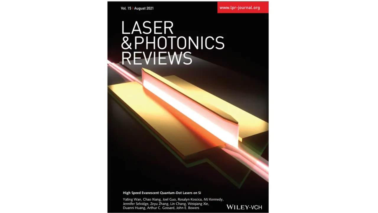
Please check the front cover paper published in Laser & Photonics Review
Y. Wan, C. Xiang, J. Guo, R. Koscica, MJ Kennedy, J. Selvidge, Z. Zhang, L. Chang, W. Xie, D.Huang, A. C. Gossard, and J. E. Bowers*, “High speed evanescent quantum-dot lasers on Si”, Laser & Photonics Reviews 2100057, 2021
